
Innovative PCB Design Services: Elevate Your Projects

In the fast-paced world of electronics, the demand for high-quality printed circuit boards (PCBs) is ever-increasing. Whether you are developing a new gadget, an industrial machine, or a medical device, the quality of your PCB can significantly impact the performance and reliability of your product. This is where innovative PCB design services come into play, offering tailored solutions that can elevate your projects to new heights.
Understanding PCB Design
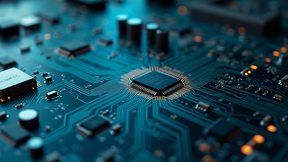
Before diving into the specifics of innovative PCB design services, it’s essential to understand what PCB design entails. A printed circuit board is a crucial component in most electronic devices, serving as the backbone that connects various electronic components. The design process involves several steps, including schematic capture, layout design, and manufacturing preparation.
Key Components of PCB Design
Schematic Capture: This is the initial phase where the electronic circuit is represented visually. Designers use specialized software to create a schematic diagram that outlines how components will connect.
Layout Design: Once the schematic is complete, the layout design begins. This involves arranging the components on the PCB and routing the connections between them. The layout must consider factors such as signal integrity, power distribution, and thermal management.
Manufacturing Preparation: After the layout is finalized, the design is prepared for manufacturing. This includes generating the necessary files and documentation that manufacturers need to produce the PCB.
The Importance of Innovative PCB Design Services
In a competitive market, having a well-designed PCB can set your product apart. Here are several reasons why investing in innovative PCB design services is crucial:
Enhanced Performance
Innovative PCB design services focus on optimizing the layout and component placement to enhance the overall performance of the circuit. For example, a well-designed PCB can reduce electromagnetic interference (EMI), improve signal integrity, and ensure efficient power distribution.
Cost Efficiency
While it may seem counterintuitive, investing in high-quality PCB design services can lead to cost savings in the long run. A well-designed PCB is less likely to encounter issues during manufacturing or operation, reducing the need for costly revisions or replacements.
Faster Time to Market
With the right PCB design services, you can streamline the development process. Experienced designers can quickly identify potential issues and provide solutions, allowing you to bring your product to market faster.
Custom Solutions
Every project is unique, and innovative PCB design services offer customized solutions tailored to your specific needs. Whether you require a compact design for a wearable device or a robust PCB for industrial applications, specialized services can deliver the right solution.
Choosing the Right PCB Design Service
Selecting the right PCB design service is critical to the success of your project. Here are some factors to consider:
Experience and Expertise
Look for a service provider with a proven track record in PCB design. Experienced designers will have the knowledge to navigate complex challenges and provide valuable insights throughout the process.
Technology and Tools
Ensure that the design service uses the latest technology and software tools. Advanced tools can enhance the design process, allowing for more accurate simulations and better overall results.
Communication and Collaboration
Effective communication is vital for a successful partnership. Choose a design service that values collaboration and is willing to work closely with your team to understand your goals and requirements.
Portfolio and Case Studies
Review the provider’s portfolio and case studies to gauge their capabilities. A diverse range of completed projects can indicate a versatile and skilled design team.
Innovative Techniques in PCB Design
The field of PCB design is constantly evolving, with new techniques and technologies emerging to improve the design process. Here are some innovative techniques that are shaping the future of PCB design:
3D PCB Design
3D PCB design allows designers to visualize the PCB in three dimensions, providing a more accurate representation of how components will fit together. This technique helps identify potential issues early in the design process, reducing the risk of costly revisions.
High-Frequency Design
As technology advances, the demand for high-frequency PCBs is increasing. Innovative design services can implement techniques to manage high-frequency signals effectively, ensuring optimal performance in applications such as telecommunications and aerospace.
Flexible PCBs
Flexible PCBs are becoming increasingly popular in various applications, from consumer electronics to medical devices. Innovative design services can create flexible PCBs that can bend and conform to different shapes, providing more design freedom.
Automated Design Tools
Automation is transforming the PCB design process. Advanced software tools can automate repetitive tasks, allowing designers to focus on more complex aspects of the design. This not only speeds up the process but also reduces the likelihood of human error.
Case Studies: Success Stories in PCB Design
To illustrate the impact of innovative PCB design services, let’s explore a couple of case studies that highlight successful projects.
Case Study 1: Wearable Health Monitor
A startup developing a wearable health monitor approached a PCB design service to create a compact and efficient PCB. The design team utilized 3D PCB design techniques to visualize the layout and ensure all components fit within the limited space. As a result, the startup was able to launch their product ahead of schedule, receiving positive feedback for its performance and design.
Case Study 2: Industrial Automation System
An established company in the industrial automation sector needed a robust PCB for a new control system. The design service implemented high-frequency design techniques to manage the complex signals involved. The final product not only met the performance requirements but also exceeded the client's expectations in terms of reliability and durability.
Future Trends in PCB Design
As technology continues to evolve, several trends are shaping the future of PCB design:
Miniaturization
The trend towards smaller and more compact devices is driving the need for miniaturized PCBs. Designers are focusing on creating smaller components and optimizing layouts to accommodate this demand.
Sustainable Design
With growing environmental concerns, there is an increasing emphasis on sustainable PCB design. This includes using eco-friendly materials and processes to minimize waste and reduce the environmental impact of PCB manufacturing.
Integration of IoT
The Internet of Things (IoT) is revolutionizing the electronics industry, and PCB design is no exception. Innovative design services are developing PCBs that can seamlessly integrate with IoT devices, enabling smarter and more connected products.
Advanced Materials
The use of advanced materials in PCB manufacturing is on the rise. These materials can enhance performance, improve thermal management, and increase the overall reliability of PCBs.
Conclusion
Investing in innovative PCB design services can significantly elevate your projects, ensuring that your electronic devices perform optimally and meet market demands. By understanding the importance of quality design, choosing the right service provider, and staying informed about emerging trends, you can position your products for success in a competitive landscape.
As you embark on your next project, consider how innovative PCB design services can help you achieve your goals. Whether you are looking to enhance performance, reduce costs, or accelerate your time to market, the right design partner can make all the difference. Take the next step in your project today and explore the possibilities that innovative PCB design can offer.
Comments